
选择你的语音
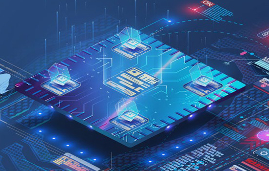
群联是能供应订制固态硬盘、NAND闪存、讯号调节及电源管理芯片的储存科技先驱
V2023_IMAGIN_SECTION6_BTN2IMAGIN+ 平台能将您对科技的想象变成现实。
无论是登陆火星或甚至是更为艰巨的科技革命,
群联专业的设计研发服务将助您达成目标。

- PCB组件原型
- 全方位的验证与测试
- ODM整合
- 供应链管理
- 最先进的研发资源共享
- NAND控制芯片ASIC设计服务
- 客制化储存解决方案
- PMIC
- Redrivers/Retimers
- AI运算模型
- AI服务解决方案
驱动、成就创新的设计服务
为甚么是IMAGIN+ 平台?
坐拥超过2000项全球专利及超过20年的产业经验,群联能提供给您符合需求的储存产品。
「只要想象得到,我们倾全力做到。」是IMAGIN+平台的核心精神和价值。

倍增竞争力
群联基于自主设计的多样IP及对研发的不懈投入,不断以超水平的各式解决方案成就我们的客户及合作伙伴。

高效精简研发流程
群联独创的资源共享平台将有效增加NAND控制器芯片及各式储存装置的分段设计及工作流程效率。

优异上市效率
群联透过维持制造流程的弹性,得以根据合作伙伴需求加速终端产出,并提升总体产品上市效率。

IMAGIN+ 案例解析
- 游戏主机
- 大型电玩机台
- 销售处理系统
- 印刷及事务机
- 工业制造
- 车载应用
-

游戏主机
客户要求
- 帧率(FPS)考虑及加载时间缩减
- 减少数据足迹
- 温控效率及相关保护措施
群联对策及解方
- 群联独家韧体算法 IO+技术™
- 特殊制程及硬件设计
- 独特用料搭配温控机制
成果
- 得以维持最低帧率并缩减达30%以上的加载时间
- 减少达60%的数据足迹
- 实现无风扇设计搭配多层次温控保护机制
-

大型电玩机台
客户要求
- 稳定帧率(FPS)
- 缩减开机时间
- 防窜改安全保护
群联对策及解方
- 群联独有系统快取技术
- 韧体调制快速开机机制
- NVMe设置厂商特有指令(Vendor Unique Command)
成果
- 得以维持最低帧率
- 减少达35%的开机和重开机耗时
- 实现特殊防骇设计
-

销售处理系统
客户要求
- 严谨要求最低效能临界点
- 降低功耗
群联对策及解方
- 针对工作负载的特殊韧体调校达成稳定I/O吞吐
- 针对工作负载的系统时钟调校及最佳效能维持
成果
- 系统数据I/O吞吐量目标达成
- 实现15%功耗缩减
-

印刷及事务机
客户要求
- 提升耐久度以确保最佳实地适用性
- 加强预防机台运作中临时断电数据保护漏洞
群联对策及解方
- 分析客户工作负载并客制韧体优化处理效能
- 韧硬件搭配实现多层快取和SSD内部进阶媒体区域划分
- 韧体客制以确保及时定存所需暂存数据
成果
- 增加超过2.5倍的储存TBW (Total Byte Written)
- 30毫秒内主机数据写入断电保护机制
-

工业制造
客户要求
- 倍数增加储存写入耐久度
群联对策及解方
- 群联独有错误修正算法(ECC)
成果
- 较原始规格3倍提升总体耐久度
-

车载应用
客户要求
- 最低不良率
- 极端温度需求
群联对策及解方
- 独特测试脚本及制程
- 群联独有韧体温控管理机制
成果
- 减少60%不良率
- AEC 车规 Grade 2 标准下可耐-40°C至105°C及 ±80°C 宽温试应能力
IMAGIN+ FAQ
是否有最小订购量(MOQ)要求或一次性工程费用(NRE Fee)?
使用Imagin+,您将得到的是Tier-1 OEM质量的全面解决方案及服务。群联不但提供ASIC设计服务,并包办包含全面可靠度测试的深度韧体客制、调校及验证,并同时为您妥善管理生产线及供应链。提供高质量解决方案的同时,群联更能根据产量规模回馈给您对应的成本节约效益。因此,群联并不预设MOQ及NRE的相关标准,而是会将您的IMAGIN+项目规模及需求,搭配上适合的合作模式及成本配置,完整为您适配及建议所需成本及资源一切相关详情。
We welcome you to consult with us to see how Phison IMAGIN+ can benefit you.
We welcome you to consult with us to see how Phison IMAGIN+ can benefit you.
群联能协助与NAND闪存无关的设计项目吗?
群联是主要专注在NAND闪存、讯号调节及电源管理解决方案的IC设计公司,但群联同时也和客户合作授权包含SerDes、混合讯号、内存接口、ECC及安全性相关等各式储存科技IP。
如何与Phison接洽IMAGIN+相关业务?
请透过网页下方连结或任何群联窗口提供您的设计需求,群联将视情况提供给您IP授权或各式芯片及模块产品客制化设计服务。
群联一般需要多少时间去开发一款客制化ASIC?
时间排程需根据IC应用及客制化复杂度而定。
群联曾有9个月内完成一个 PCIe 4.0 SSD ASIC开发的先例, 但可想象更加复杂的设计将耗时更多,确切工作时间轴需视您的需求方可详细评估。
群联在加速项目的经验有目共睹,ASIC项目皆会在下线前提早使用FPGA模拟仿真设备环境搭配成熟的韧体进行持续验证。过去多数的第一次投片皆已成熟至可上市的程度。
群联曾有9个月内完成一个 PCIe 4.0 SSD ASIC开发的先例, 但可想象更加复杂的设计将耗时更多,确切工作时间轴需视您的需求方可详细评估。
群联在加速项目的经验有目共睹,ASIC项目皆会在下线前提早使用FPGA模拟仿真设备环境搭配成熟的韧体进行持续验证。过去多数的第一次投片皆已成熟至可上市的程度。
群联设计服务的优势为何?
- 引领业界的科技研发实力、产品竞争力和卓越执行力
- 大量可授权自有IP及研发资源
- 高效率、低风险的产品上市规划能力
请分享一些群联提供的客制化设计案例?
ASIC客制案例:
- 各式PCIe特色功能
- 单一根I/O 虚拟化 (SR-IOV) 物理机能(PF)和虚拟机能(VF)
- 低功耗和时钟树(clock tree)优化
- 安全性应用
- 错误修正码(ECC)引擎
- 规章适配性 (Compliance)
- 互操作性 (Interoperability)
- 错误排除设计
韧体客制案例:
- 工作负载和用户体验优化
- 高温降速设计
- 低耗能模式优化
- 安全性应用
- 耐久度及数据储存能力
- NVMe设置厂商特有指令(Vendor Unique Command)
- 产品和机种编号
群联针对IP授权能提供那些档案和参考数据?
- 使用者说明
- 行为模型和RTL代码
- 布线后网表汇整
- 标准延迟格式(SDF)文件
- Libray (LIB)
- Frame view (LEF)
- 相关测试脚本
- 更多其他相关信息
我要如何开启属于我的IMAGIN+计划?
非常简单! 请使用下方连结和我们联系:
- 告诉我们您期望的产品概念
- 我们将提供您一个初步的时程和成本估算结果
- 开始纪录工作范围和执行细节